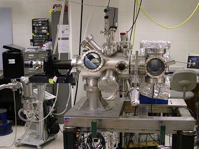
In the post titled “Nanotechonology. Introduction” I mentioned that the development of the scanning tunneling microscope played a fundamental role in the progress of nanotechnology, so let’s learn a little more about it and how it works.
The scanning tunneling microscope (STM) was developed by Gerd Binning and Heinrich Rohrer in 1981 at IBM laboratories in Zurich (Switzerland), for which they were awarded the 1986 Nobel Prize in Physics.
The scanning tunneling microscope (STM) was developed by Gerd Binning and Heinrich Rohrer in 1981 at IBM laboratories in Zurich (Switzerland), for which they were awarded the 1986 Nobel Prize in Physics.
Both the STM and the AFM (atomic force microscope) are classified as scanning probe microscopy instruments, but the first is far more powerful and is able to handle and observe atoms and molecules with higher resolution.
The STM is used to take images of conductive surfaces at an atomic scale of around 2 Å (2*10-10 m). It can also modify the examined sample by manipulating individual atoms, setting off chemical reactions and originating ions by replacing electrons from certain atoms with others.
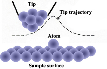
The scanning tunneling microscope is a non-optical microscope (it does not use rays of light to take us down to nano-dimensions) whose operation is based on quantum mechanic principles. An extremely fine probe is positioned over the specimen under study at a distance of the diameter of an atom, applying a voltage between them. Depending on the characteristics of that voltage, the electrons can jump from one side to the other by tunneling effect[1], producing a weak current flow, known as “tunneling current”, whose value is approximately a few picoamperes (1 pA = 10-12 A).The stylus probe is very sharp, with a tip formed by a single atom. It scans the surface at a very slow speed, raising and lowering (by a piezoelectric mechanism[2] to control its level) in order to maintain a constant distance and signal, which permits the inspection of the tiniest detail of the sample that is being scanned.
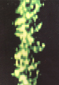
The vertical movement of the stylus is registered allowing the inspection of the surface structure atom by atom, producing a contour map of the surface generated by a computer.
The vertical movement of the stylus is registered allowing the inspection of the surface structure atom by atom, producing a contour map of the surface generated by a computer.
Electrical insulating materials cannot be analysed by this technique because, as their electrical charges do not flow freely it consequently makes it impossible to conduct any kind of current between them and the probe tip.
Although these instruments show an optimal operation examining conductive materials, they can also provide topographical characterisations of organic molecules such as DNA or proteins.
This type of microscope plays an important role in physics, specifically in the study of semiconductor surfaces and in the field of microelectronics. It also proves to be important in chemistry, studying superficial reactions like catalysis or in nanoscale chemistry laboratories, where the analysis of the physical structure of synthetic chemical compounds and material defects is essential.
[1] The tunnel effect consists in those quantum particles (electrons in this case) that in spite of the fact of not having enough kinetic energy (energy associated with body motion), they penetrate and cross a space that, in principle, would be impossible, due to the presence of a potential barrier that should block their flow.
[2] Materials that are deformed through expansion or contraction, under the action of an electric field.
[2] Materials that are deformed through expansion or contraction, under the action of an electric field.
Sources: http://education.mrsec.wisc.edu/130.htm
http://www.nobelprize.org/educational/physics/microscopes/scanning/
http://hoffman.physics.harvard.edu/research/STMintro.php
http://www.uwec.edu/Matsci/center/instrumentation/
http://www.nobelprize.org/educational/physics/microscopes/scanning/
http://hoffman.physics.harvard.edu/research/STMintro.php
http://www.uwec.edu/Matsci/center/instrumentation/


Your opinion matters